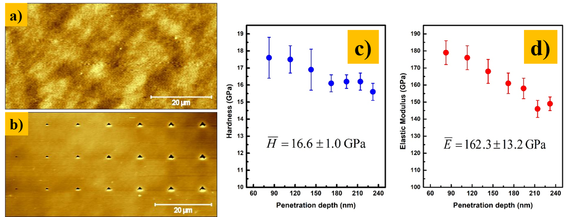
Micro-/nano-indentation test, performed on a SOI wafer sample
a) 70×70 µm2 2D topography image of SOI sample recorded BEFORE performing the micro-/nano-indentations; b) 75×75 µm2 2D topography image of SOI sample recorded AFTER performing the micro-/nano-indentations; c) the mean value of the Hardness parameter calculated for SOI sample; d) the mean value of the Elastic Modulus parameter calculated for SOI sample
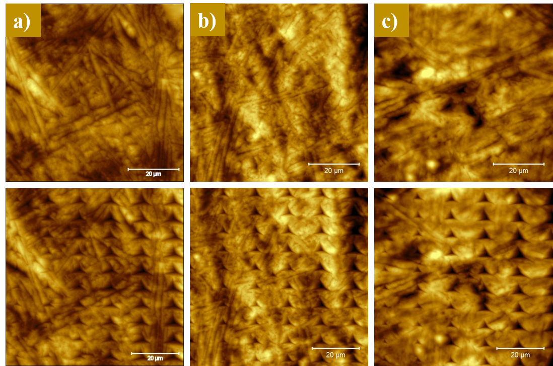
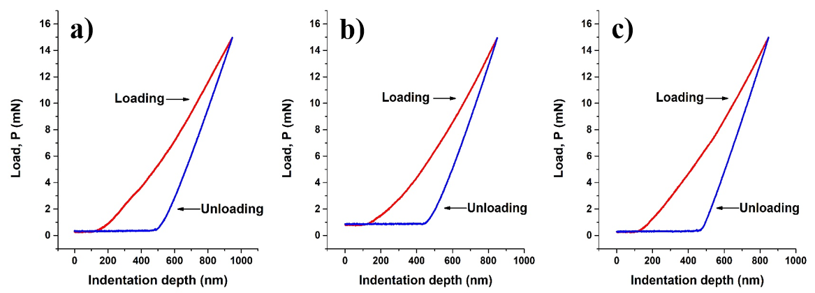
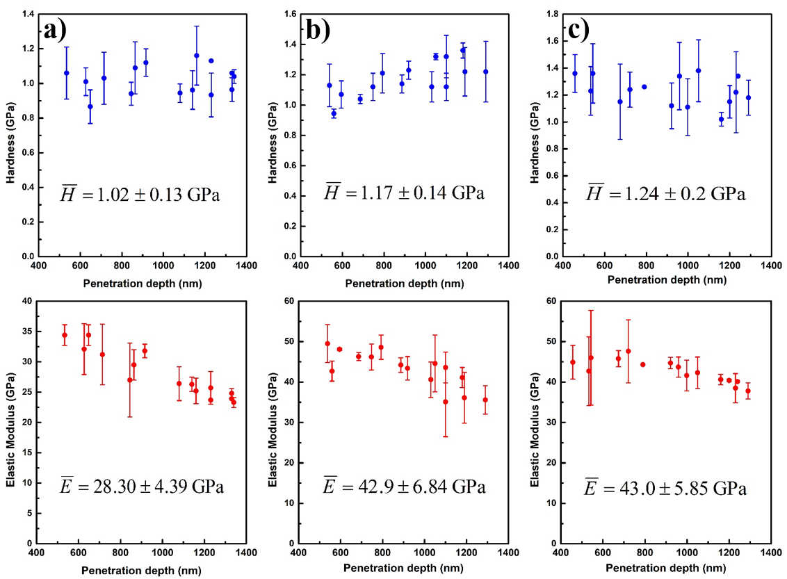
Micro-/nano-indentation tests, performed on TiZr nanocoatings
70×70 μm2 and 75×75 μm2 2D topography images of TiZr nanotubes (prepared in different conditions), recorded before (top row) and after (bottom row) performing the indentation measurements
Representative loading curves recorded at approximately 15 mN load for TiZr samples
The mean values of elastic modulus and hardness parameters calculated for TiZr samples, and plotted versus penetration depth