DESCRIPTION:
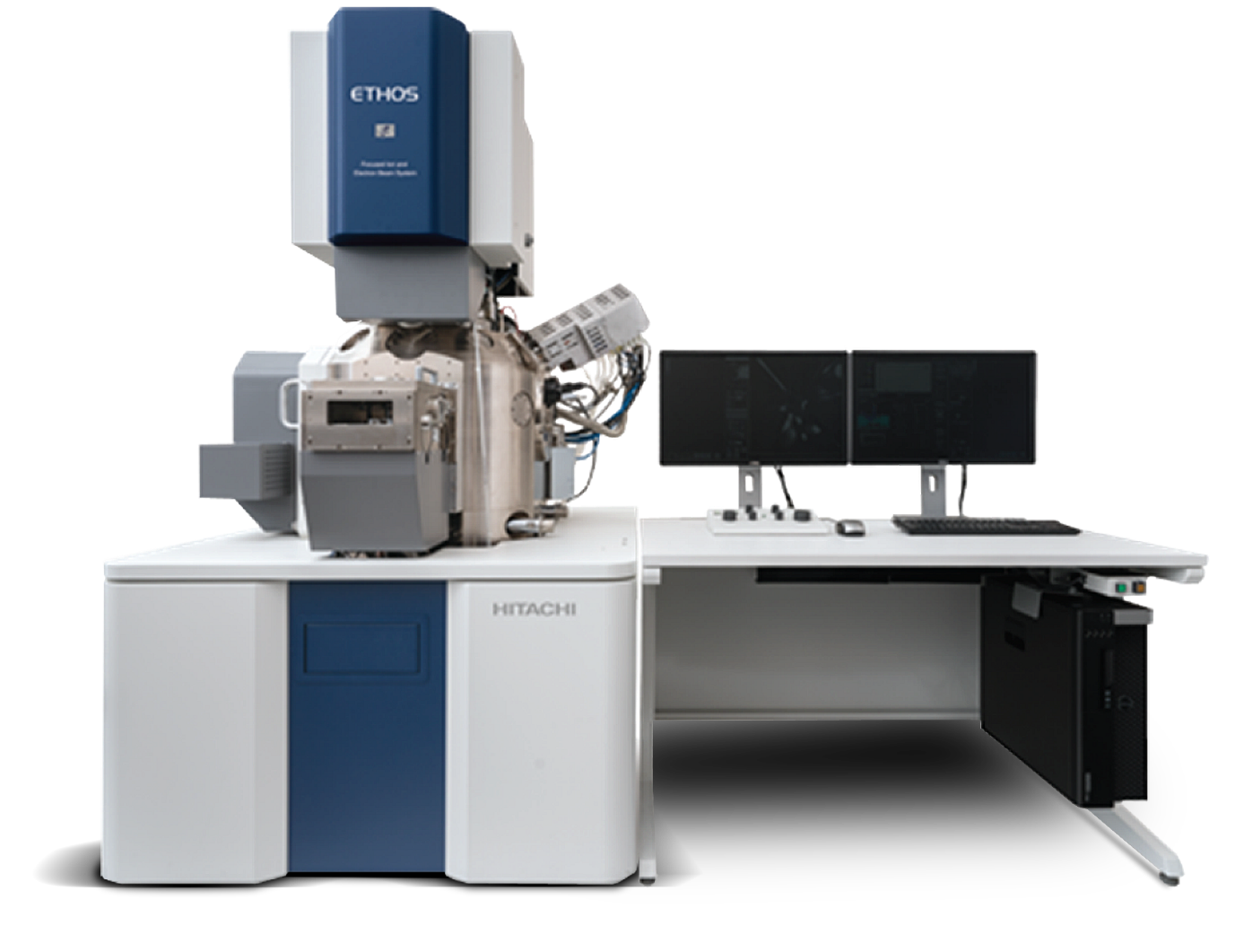
Hitachi ETHOS NX5000 is a complex system that combines a high-intensity cold-cathode field emission electron gun technology with a newly developed magnetic/electrostatic compound lens (or dual-mode lens). The NX5000 system incorporates a FIB column for sample processing and a SEM column for high-magnification observation in a single specimen chamber. A two-column system allows for fine structure and compositional observation of specific regions along the specimen plane as well as subsurface regions of interest. In addition, the system incorporates an Ar gun in order to reduce the Ga implantation, which may occur in cross-sectional processing via FIB.
The FIB-SEM system is used in a wide variety of application fields, such as semiconductors, nanotechnology, materials science, medicine, and biology, for cross-sectional observation and analysis of samples, as well as preparation of lamella TEM samples. The instrument is equipped with a newly developed large sample stage allowing observation and processing of 150 mm diameter samples in their entirety. In addition, the system can provide the elemental analysis of the samples with the EDS detector (Oxford Instruments ULTIM MAX with 65 mm2 detector area with 1.1 steradian).
Energy Dispersive X-ray – EDX
EDX is an analytical technique used for the elemental analysis or chemical characterization of a sample. The equipment is provided with a Silicon Drift Detector (SDD) available on the market, with an area of 65 mm2 for advanced nano-analysis. Benefits of the SDD include:
- High count rates and processing
- Better resolution than traditional Si (Li) detectors at high count rates
- Lower dead time (time spent on processing X-ray event)
- Faster analytical capabilities and more precise X-ray maps or particle data collected in seconds
- Ability to operate at relatively high temperatures, eliminating the need for liquid nitrogen cooling
Type of analysis:
- Chemical and structural characterization of the samples;
- Structure investigations of semiconductors;
- Morphological research;
Technical details
SIM resolution: 4 nm @ 30 kV, 60 nm @ 2 kV (Edge resolution)
Accelerating voltage: 0.5 kV – 30 kV
Beam current: 100 nA
Ion source: Ga Liquid Metal Ion Source
SEM resolution: 1.5 nm @ 1 kV, 0.7 nm @ 15 kV
Accelerating voltage: 0.1 kV – 30 kV
Max. beam current: 10 nA
Electron source: Cold cathode field emission
Detectors:
- In-column secondary electron detector, SE (U)
- In-column backscattered electron detector, BSE (U)
- In-column backscattered electron detector, BSE (L)
- Chamber mounted secondary electron detector, SE (L)
- EDX
Key features:
- High-Performance FE-SEM Column with Dual Lens Mode (HR mode: semi-in-lens, FF mode: time sharing mode)
- High-Throughput Material Processing: ultra-fast processing with high ion-current density (Max. beam current: 100 nA)
- Microsampling System: TEM sample preparation for uniform lamellas at any orientation
- Triple-Beam Capable, Delivering Advanced Quality Results: low-acceleration noble-gas ion-beam material processing, innovative functions reduce Ga ion-related and other milling artifacts.
- Large Multi-Port Chamber and Stage for Various Applications: deposition of different gases, (W, Pt, C), large sample size, capable system with exceptional stage stability
- Full range enhanced long-distance tracking (155 x 155mm)
Stages:
- Standard stage
- Dedicated stage for circular sample with a surface up to 120 mm
- Dedicated stage for rectangular sample with a surface up to 150 mm