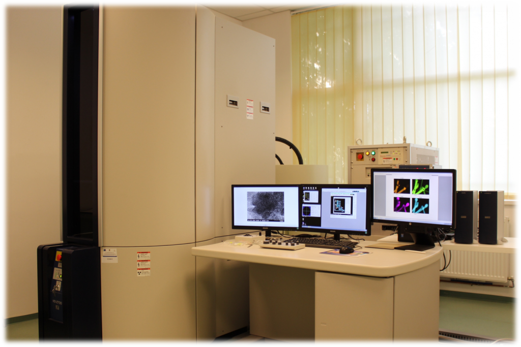
DESCRIPTION:
The equipment allows the morphological characterization at micro- and nanometric level for a large range of nanomaterials and micro/nanocomponents of various devices. The system is equipped with scattered electrons (SE), Z contrast (ZC) and transmission electrons (TE) detectors, able to perform at ultra-high level resolution (0.5 nm – SEM mode and 0.14 nm – STEM mode) at the same location of the specimen.
Scanning Transmission Electron Microscope (STEM) equipped with real time EDX (Energy Dispersive X ray) with Silicon Drift Detector (SDD) and electron diffraction analytical techniques.
Nano-diffraction
For studying the structure of nanoparticles as a function of their size requires a correlation between the image and the diffraction pattern of single nanoparticles. Nano-beam diffraction technique is able to identify the crystalline structure at nanometer level, even when nanoparticles are randomly oriented on an amorphous substrate.
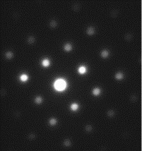
Nano-diffraction pattern of single crystal gold nanoparticle.
Energy Dispersive X-ray – EDX
EDX is an analytical technique used for the elemental analysis or chemical characterization of a sample. The equipment is provided with one of largest Silicon Drift Detector (SDD) available on the market with an area of 150 mm2 for advanced nano-analysis and delivers more than double the speed of any other detector.
Benefits of the SDD include:
- High count rates and processing
- Better resolution than traditional Si(Li) detectors at high count rates
- Lower dead time (time spent on processing X-ray event)
- Faster analytical capabilities and more precise X-ray maps or particle data collected in seconds
- Ability to operate at relatively high temperatures, eliminating the need for liquid nitrogen cooling