Nano-manipulation System and electrical characterization in situ in the Scanning Electron Microscope (SEM)
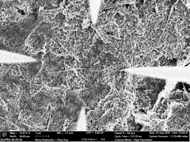
The nano-manipulation system has four heads for gripping, handling and determining the electrical properties (I vs V curves in the voltage range: -10 V / +10 V) of the various nanomaterials (nano-tubes, nano-wires, nano-belts, etc.) and micro / nano-devices of interest.
The manipulation of objects of micrometric and nanometric dimensions is critical nowadays due to the rapid development of nanotechnology in the last three decades.
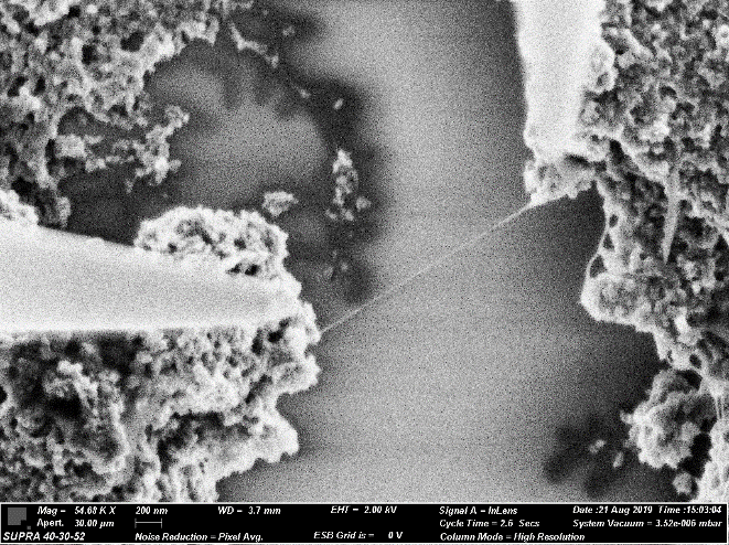
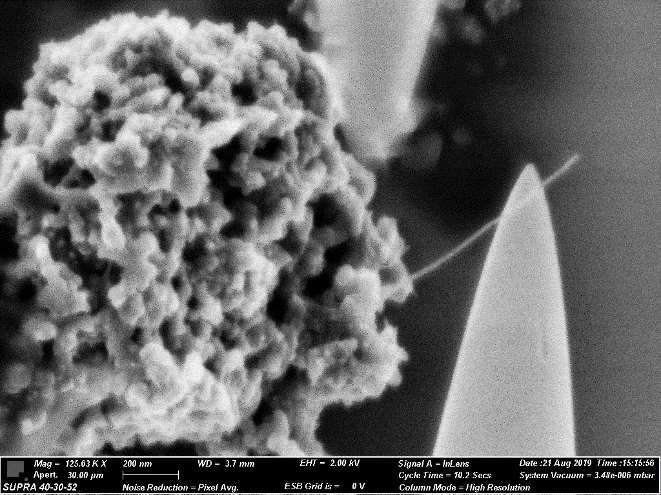
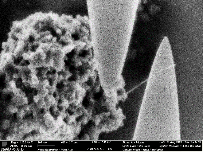
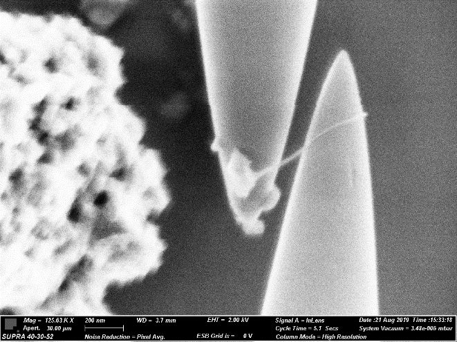
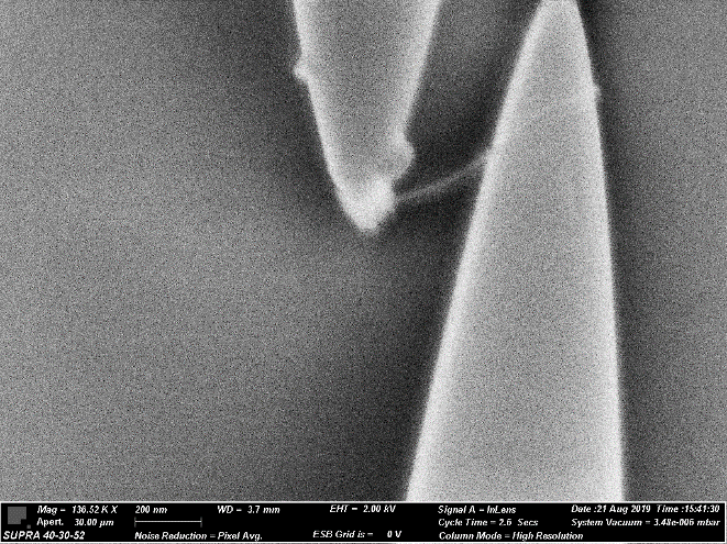
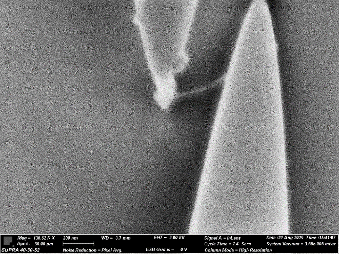
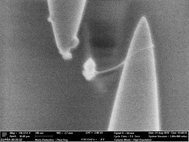
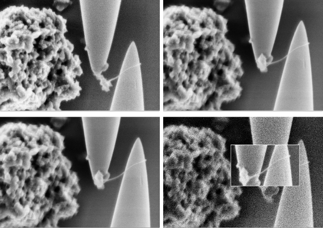
Manipulation of a SWCNTs Bundle
The combination of Scanning Electron Microscopy and advanced micro/nanomanipulation technology allows real-time and in situ study of the electrical properties of individual 1D (nanowires/nanotubes) and 2D (graphene) nanostructures, allowing the correlation of their properties with a wide range of applications.
The hybrid system simplifies the construction and assembly of nanometer-sized blocks in nano-devices. Pre-synthesized nanotubes or nanowires can be integrated, using the nanomanipulation system, into different structures to obtain, for example, nano-FETs. Mechanical nanomanipulation is very precise in the incorporation of a single nanotube/nanowire, as compared to other methods of obtaining FET nanodevices.
In addition, the study of the electrical properties of metallic or semiconductor nanomaterials is of particular interest due to the wide field of applications in nano-electronics and nano-devices. The electrical resistance of the nanowire evaluated by the I-V curves determines the performance of the entire device, therefore it is necessary to study the properties of the individual nanowires.
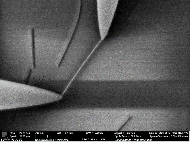
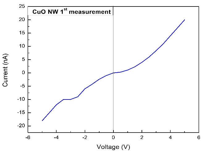
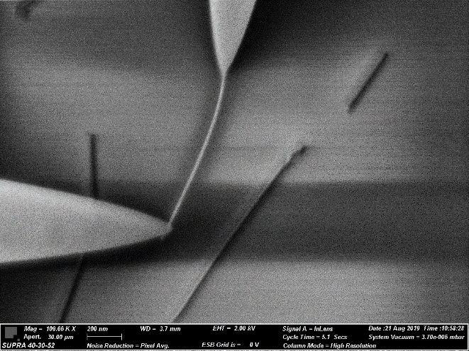
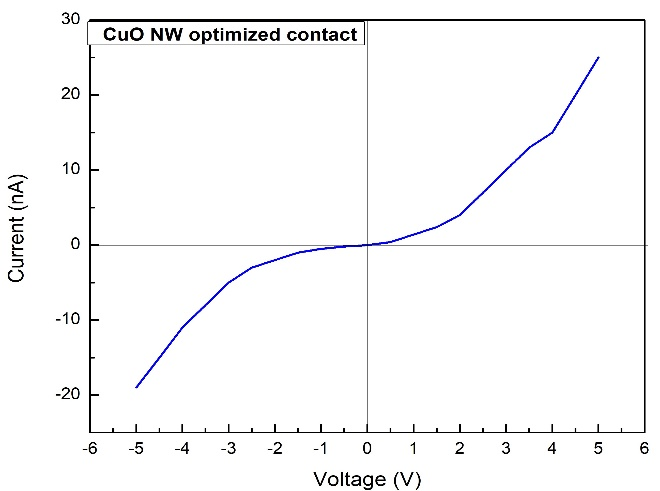
Electrical Characterization of a single CuO Nanowire
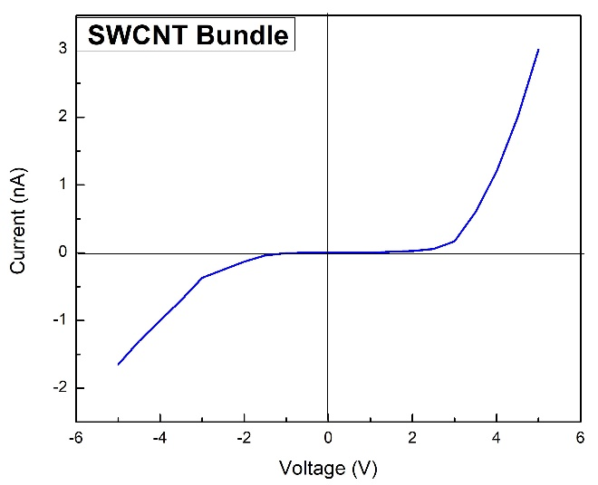
Electrical Characterization of a SWCNTs Bundle
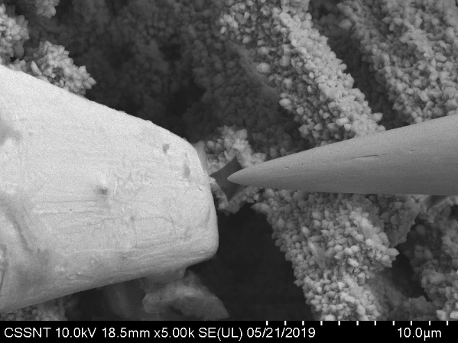
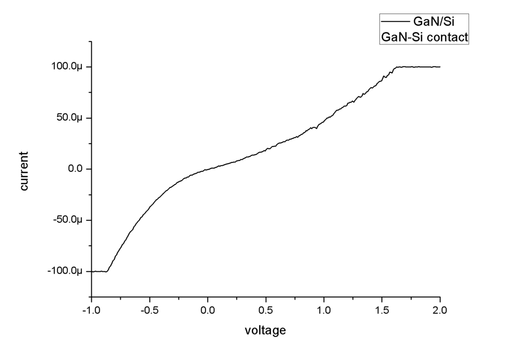
Electrical Characterization GaN Crystal – Si pillar junction
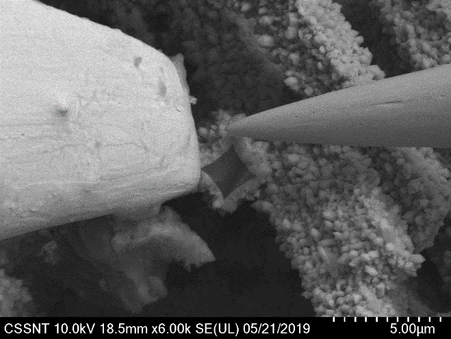
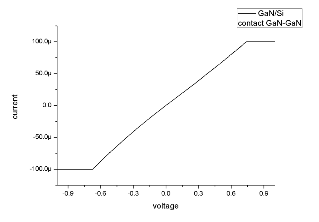
Electrical Characterization GaN – GaN Crystals
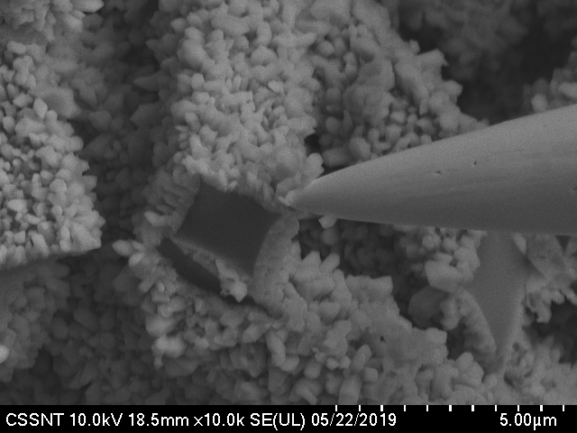
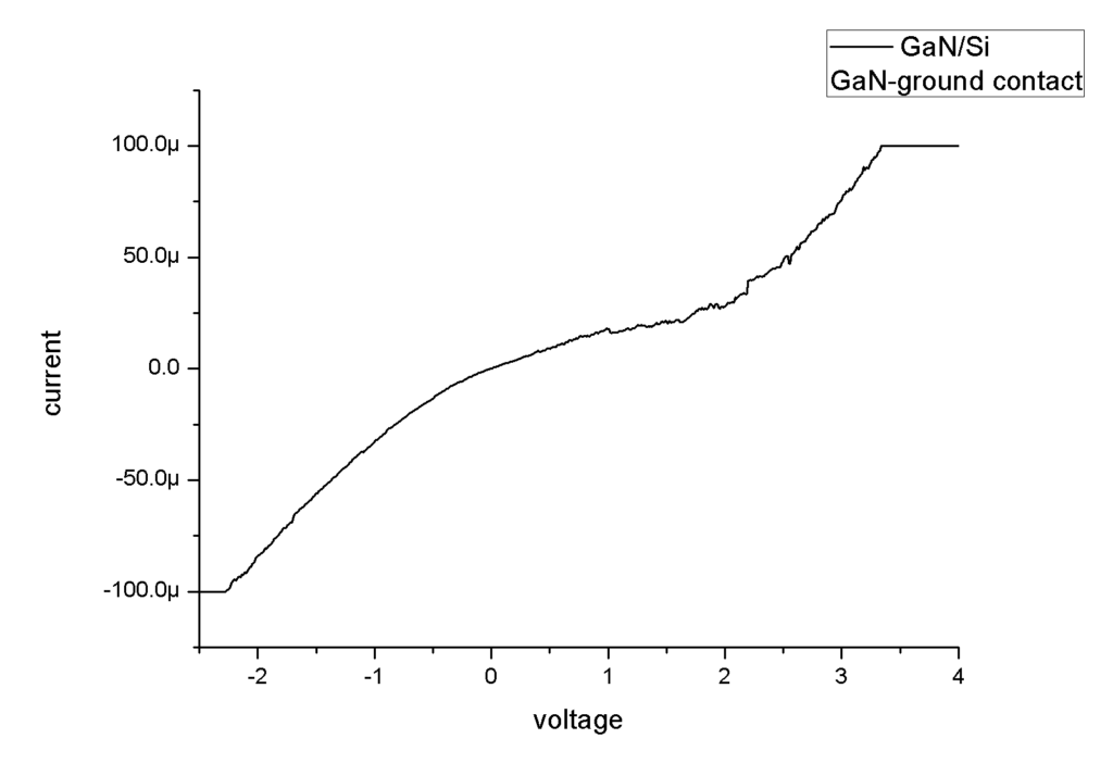
Electrical Characterization GaN Crystal – ground
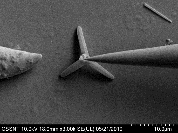
Piezoelectric measurement on GaN tetrapod
The results obtained on the GaN structures are in collaboration with the Technical University of Moldova and the Academy of Sciences of Moldova.
The nano-manipulation and mechanical characterization system in the scanning electron microscope (SEM)
The Nano-indentation System is used for specialized indentation measurements at nano level, of nanomaterials and micro / nano-devices of interest, applying forces in the range 1- 360 µN.
Nanoindentation is, to date, the only viable approach for measuring the mechanical properties of nanomaterials due to their extremely small dimensions. The combination of the electron microscope with the nano-indentation system allows the direct observation of the behaviour of the nanomaterial. Cracks generated by mechanical tests and their propagation can be detected in real time by correlating them with the applied mechanical force. Understanding the properties of individual nanostructures, such as the deformation mechanism and the mechanical properties (modulus of elasticity and hardness), will help to control the final structure.
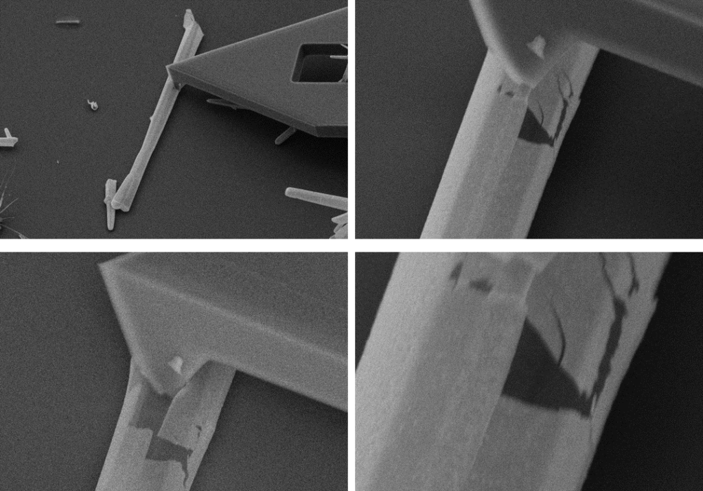
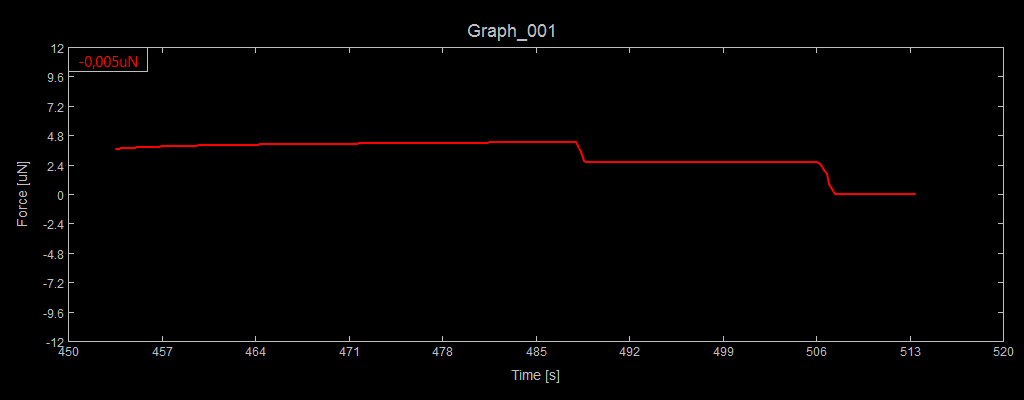
Indentation of a GaN Nanotube
