DESCRIPTION:
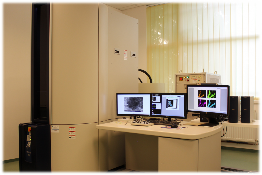
The HD2700 model from Hitachi is a scanning transmission electron microscope (STEM) coupled with secondary electron mode (SEM) imaging capability. It is a complex system capable of performing imaging and morphological/topographical analyses in three different modes, namely, secondary electron mode (SEM), ZC-phase contrast, and scanning transmission electron mode (STEM). The atomic resolution in the SEM mode is 0.5 nm, and in the STEM mode is 0.14 nm.
The system has a cold (cathode) field emission electron gun type (C-FEG) and can operate at different accelerating voltages: 80, 120, and 200 kV. It is equipped with an EDS detector from Oxford Instruments, model X-MaxN 100 TLE with 100 mm2 detector area, with 2 steradians in order to provide elemental analysis of the samples.
On the other hand, the tool’s configuration and the attachments that allow the cryogenic device (915 Gatan Double tilt liquid nitrogen cryo-transfer holder) qualify the STEM for reliable cryo analysis on sensitive materials.
Nanodiffraction
Studying the structure of nanoparticles as a function of their size requires a correlation between the image and the diffraction pattern of single nanoparticles. Nano-beam diffraction technique can identify the crystalline structure at the nanometer level, even when nanoparticles are randomly oriented on an amorphous substrate.
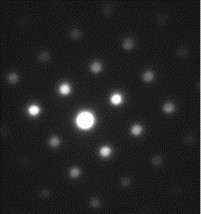
Nano-diffraction pattern of a single crystal gold nanoparticle.
Energy Dispersive X-ray – EDX
EDX is an analytical technique used for the elemental analysis or chemical characterization of a sample. The equipment is provided with one of the largest Silicon Drift Detector (SDD) available on the market, with an area of 100 mm2 for advanced nano-analysis and delivers more than double the speed of any other detector.
Benefits of the SDD include:
- High count rates and processing
- Better resolution than traditional Si (Li) detectors at high count rates
- Lower dead time (time spent on processing X-ray event)
- Faster analytical capabilities and more precise X-ray maps or particle data collected in seconds
- Ability to operate at relatively high temperatures, eliminating the need for liquid nitrogen cooling
Type of analysis:
- Chemical and structural characterization of nanomaterials;
- Structure investigations of semiconductors;
- Organic/biological nanomaterials;
Technical details
Camera/detectors:
- Charged Couple Device (Hitachi CCD camera with 30 frames/s)
- High Angle Annular Dark Field (HAADF), Bright Field (BF), and Surface Electron (SE) – Detectors
- EDX
Holders:
- Single and double tilt holder
- Cryo-Holder (LN2)