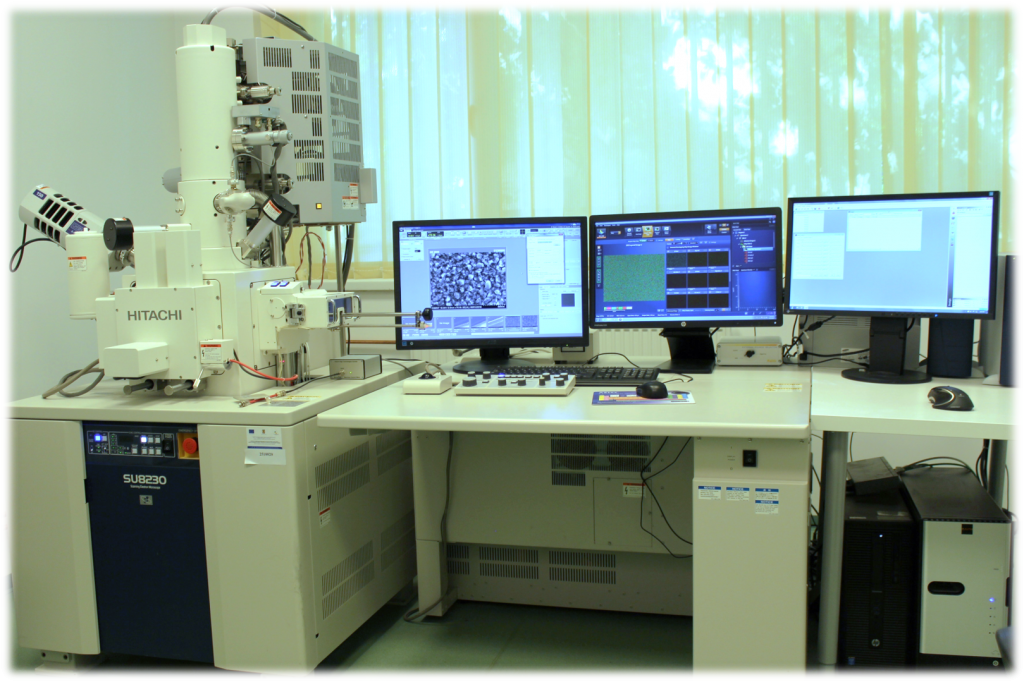
DESCRIPTION:
SEM is used to generate high-resolution (<0.7 nm) images of object shapes (SEI), to show spatial variations in chemical compositions: acquiring elemental maps or spot chemical analyses using EDS, discrimination of phases based on mean atomic number (commonly related to relative density) using BSE, and compositional maps based on differences in trace element.
SEM is also used to identify phases based on qualitative chemical analysis and crystalline structure. Backscattered electron images (BSE) can be used for rapid discrimination of phases in multiphase samples.
Scanning Electron Microscope (SEM) equipped with:
- EDX (Energy Dispersive X-ray) System is a leading provider of innovative materials characterization systems encompassing Energy Dispersive Spectroscopy (EDS). EDX products include standalone tools, integrated tools for EDS and a free-standing Micro-XRF bench-top elemental analyser providing small and micro-spot X-ray analysis and mapping. The application specific for device is Particle Analysis, Thin Film characterization, and Mineral Liberation Analysis.
- E-Beam Lithography System (EBL) The SEM-EBL system facilitates the fabrication of submicron devices or nanometer sized components due to the use of a very narrow electron beam (nanometer size) and of the selected design involving the equipment software. The desired geometrical configuration is thus created on the resist layer deposited onto the material. The technical limit of light diffraction (specific to photolithography) has been surpassed by the current SEM-EBL nanolithography technique. The simultaneous morphological and topological analysis of the built geometrical nanostructures is also possible due to the SEM microscope present in the system.