English
 Română (Romanian)

Expert Metrology Course 2026
Advanced Characterization and Metrology Techniques for Semiconductor Materials, Structures and Devices
Center for Surface Science and Nanotechnology (CSSNT)
National University of Science and Technology
POLITEHNICA Bucharest, Romania
Course description
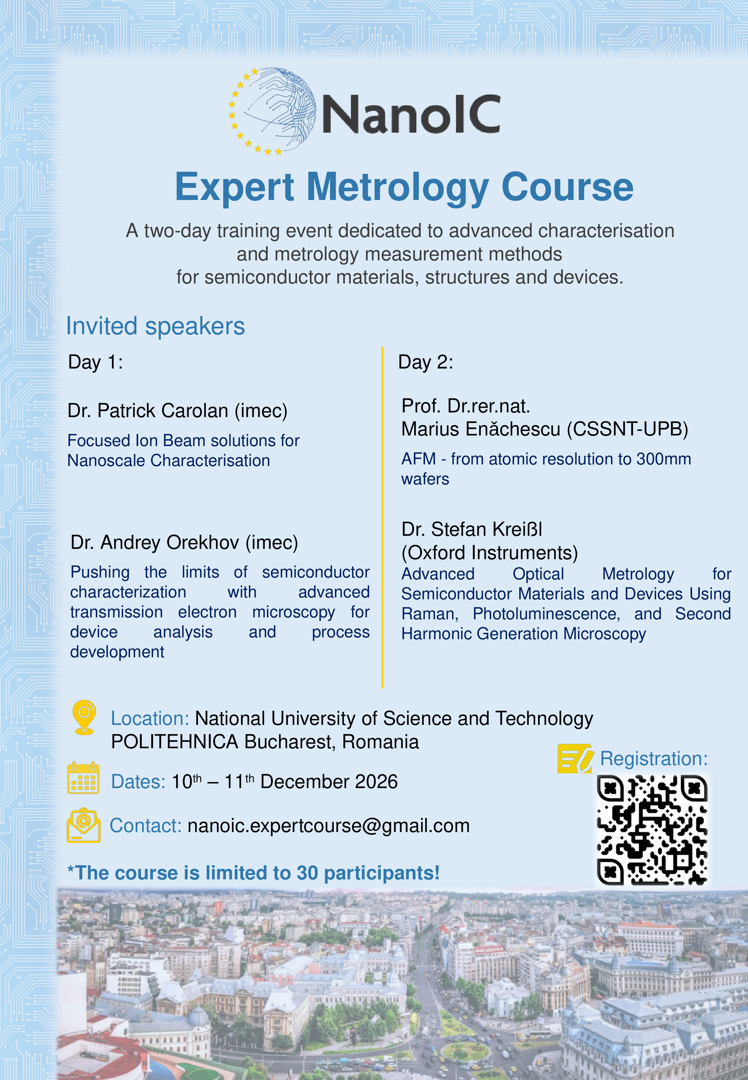
The Expert Metrology Course is a two-day training event dedicated to advanced characterization and metrology measurement methods for semiconductor materials, structures, and devices. Organized by the Center for Surface Science and Nanotechnology (CSSNT) and hosted by the National University of Science and Technology POLITEHNICA Bucharest, the course brings together experts to share their knowledge and practical experience with researchers, professors and PhD students.
The course will cover advanced techniques: SEM-FIB, STEM-EDX-EELS, AFM, AFM-IR, SHG, PL and µRaman, with emphasis on their applications in semiconductor research and development.
Participants will learn about the operating principles, capabilities, and limitations of the selected metrology methods, as well as appropriate measurement strategies, data interpretation, and common sources of uncertainty. The workshop will also demonstrate how complementary characterization techniques can address complex materials and device-related questions.
Date and location
Date: 10–11 December 2026 (two full days)
Venue: National University of Science and Technology POLITEHNICA Bucharest
Address: Splaiul Independenței 313, Sector 6, Bucharest, Romania
Two-day programme
Day 1 — 10 December 2026: Lectures on sample preparation using SEM-FIB and atomic and nanoscale imaging using STEM-EELS.
Day 2 — 11 December 2026: Surface science topics, including AFM, AFM-IR, SHG and µRaman.
The theoretical sessions will be supported by laboratory visits planned for each module, giving participants the opportunity to discuss their research questions directly with specialists in the field.
Target audience
The course is intended for R&D professionals, academic researchers, professors and PhD students working on advanced semiconductor technologies and related processes.
Registration and practical information
Participation is free of charge, but prior registration is required. The number of places is limited to 30 participants.
Registration deadline: 1 November 2026. Registration may close earlier if all places are filled.
Participant confirmation: 10 November 2026.
Register here: NanoIC Expert Metrology Course — Registration form
Participants are responsible for arranging and covering their own travel and accommodation. No travel or accommodation reimbursement is foreseen.
For registration assistance or practical questions, please contact: nanoic.expertcourse@gmail.com
NanoIC Pilot Line
The course forms part of NanoIC’s work on education, training and skills development. Through these activities, NanoIC supports Europe’s semiconductor community by connecting researchers and students with specialist knowledge and practical expertise.
Course flyer